
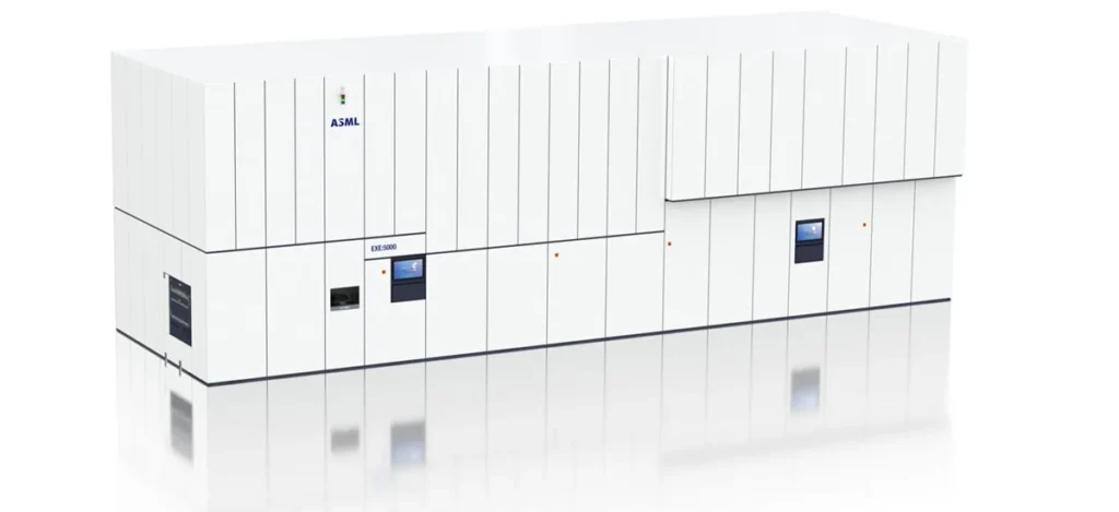
ASML High-NA EUV is moving from a technology demonstration into the production plans of the world’s most important chipmakers, strengthening ASML’s grip on the most advanced part of semiconductor manufacturing.
Intel is already using High Numerical Aperture extreme ultraviolet lithography in high-volume manufacturing on selected layers of its Intel 18A process. TSMC and Samsung have now committed to the broader ecosystem needed for future deployment, while memory manufacturers including Samsung and SK Hynix are preparing to use the technology later in the decade. The shift matters because High-NA EUV is designed to print smaller features with fewer patterning steps than today’s most advanced EUV systems.
ASML’s next-generation scanners are also among the most expensive pieces of industrial equipment ever produced. Reuters reports that current EUV systems cost around $200 million each, while High-NA tools can reach roughly $400 million. That price once raised questions over whether leading foundries would adopt the technology quickly. Those doubts are fading as chipmakers align around both the scanners and the photomask infrastructure required to use them efficiently.
What is High-NA EUV?
High-NA EUV is the next major step in extreme ultraviolet lithography, the process used to print tiny circuit patterns onto silicon wafers. The “NA” stands for numerical aperture, a measure that affects how finely the optical system can resolve features. Conventional EUV systems use a numerical aperture of 0.33. ASML’s High-NA platform increases that to 0.55.
That change allows the system to resolve significantly smaller structures. Intel has said High-NA can print features up to 1.7 times smaller than 0.33-NA EUV and potentially deliver up to 2.9 times greater two-dimensional density in appropriate layers. Reuters describes the resolution improvement as roughly 40% smaller printable features.
The practical value is not simply smaller transistors. Advanced chipmakers often use multiple exposures and complex patterning techniques to create features that a single exposure cannot resolve. Those extra steps add cost, time, process complexity and opportunities for manufacturing defects. A higher-resolution lithography system can eliminate some of that complexity on selected layers.
Intel is already using High-NA in production
Intel has been ASML’s earliest major customer for High-NA EUV. In 2024 it installed the industry’s first commercial TWINSCAN EXE:5000 system at its Oregon development facility. That first-mover strategy has now progressed into manufacturing.
On September 7, 2026, Intel Foundry and ASML said that more than one million wafers had been processed across tool qualification, research, development and volume production. Intel is using High-NA on selected layers for a subset of Core Ultra Series 3 processors, code-named Panther Lake.
Intel also said overlay, throughput and availability are meeting its expectations, and that Intel 18A layers produced with High-NA are delivering performance comparable to or better than equivalent layers patterned with ASML’s existing NXE EUV platform.
This is an important milestone because it moves High-NA beyond laboratory demonstrations. Semiconductor manufacturers are conservative about introducing new lithography systems because a single problem can affect yield across extremely expensive wafers. Production use gives other foundries evidence that the platform can operate at industrial scale.
TSMC’s support removes a major adoption question
TSMC was previously cautious about the economics of High-NA. The Taiwanese foundry dominates production of the world’s most advanced logic chips, including processors for companies such as Apple, Nvidia and AMD, so its adoption decisions have enormous influence over the semiconductor equipment market.
That caution has shifted. TSMC and ASML announced an initiative on September 8 to lead the semiconductor industry’s transition toward larger 12-inch photomasks for High-NA EUV. The companies said the initiative targets a pilot line by 2031 and full lithography-system readiness for advanced-node manufacturing by 2033.
The agreement does not mean TSMC will wait until 2033 to use High-NA. Production can begin with current 6-inch masks. The larger-mask program is intended to remove a structural limitation of the first High-NA systems and improve economics as the technology scales.
The photomask problem High-NA needs to solve
High-NA’s stronger optics create a smaller exposure field than conventional EUV. That creates what the industry calls the half-field challenge: very large chip designs may not fit into one exposure using today’s standard mask format.
There are several ways to work around this. Designers can arrange their layouts to fit the available field, or manufacturers can stitch multiple exposures together. Intel has developed stitching techniques and design-kit support for customers that want to use High-NA before larger masks arrive.
The long-term solution being pursued by ASML, TSMC, Intel, Samsung and other ecosystem partners is a larger photomask. Moving from the industry’s decades-old 6-inch mask format to a 12-inch format would allow High-NA systems to expose larger areas while preserving their resolution advantage.
ASML and TSMC say the larger format should improve fab productivity, reduce chipmaking costs and remove some of the constraints associated with stitching. That transition is technically significant because photomasks are supported by a large ecosystem of inspection tools, automation systems, materials, electronic-design software and handling equipment. The scanner itself is only one part of the change.
Samsung is preparing High-NA for advanced memory
Samsung Electronics has also joined the 12-inch photomask initiative. In a September 8 announcement, Samsung and ASML said they were expanding their strategic collaboration around High-NA EUV and next-generation semiconductor manufacturing.
Samsung plans to adopt High-NA for future DRAM manufacturing, making memory an important second market alongside advanced logic. That matters because the artificial-intelligence boom is increasing demand not only for GPUs and CPUs but also for high-bandwidth and high-performance memory. More precise lithography can help memory manufacturers continue increasing density and performance.
Reuters reports that Samsung and SK Hynix are targeting High-NA deployment from 2028. If those schedules hold, ASML’s customer base for the platform will expand across the main categories of leading-edge semiconductor manufacturing.
Why ASML’s position is so unusual
ASML already holds a unique position in the semiconductor supply chain. It is the only company that sells EUV lithography systems at commercial scale. Competitors Nikon and Canon remain active in other lithography segments, and China is investing heavily in domestic semiconductor equipment, but no competing supplier currently offers an equivalent production EUV platform.
Reuters estimated ASML’s broader lithography-market share at 94% in 2025. High-NA gives the Dutch company another generation of technology at the center of advanced-node manufacturing.
This matters strategically because almost every leading AI processor depends, directly or indirectly, on ASML equipment. Nvidia does not manufacture its own chips; TSMC produces most of them. Apple also depends heavily on TSMC. Intel and Samsung operate their own fabs. Despite different business models, all of these companies operate within a manufacturing ecosystem where lithography capability sets fundamental limits on transistor scaling.
The economics are still challenging
High-NA’s technical advantages do not automatically make it economical for every layer of every chip. A scanner costing around twice as much as a conventional EUV system must save enough process steps, improve enough yield or enable enough additional scaling to justify its cost.
Foundries will therefore use a mix of tools. Intel has repeatedly said it expects conventional EUV and High-NA EUV to coexist. Some layers will benefit from 0.55-NA optics; others will remain cheaper and easier to manufacture with existing equipment.
Throughput is another major factor. A lithography scanner is valuable only if it can process enough wafers while maintaining extremely tight overlay and defect specifications. ASML’s EXE:5200B generation is designed to increase output compared with the first EXE:5000 development systems, and Intel has reported progress toward industrial performance levels.
What High-NA means for AI chips
The immediate connection to artificial intelligence is manufacturing density. AI accelerators continue to grow in transistor count and complexity. Advanced lithography helps foundries produce denser logic, while improved memory processes support faster data movement around those processors.
However, modern AI chips are also pushing against another limit: physical die size. Large GPUs and custom accelerators can approach the maximum area that lithography equipment can expose in one field. This is why mask size, reticle limits, chiplets and advanced packaging are increasingly important alongside transistor scaling.
The industry is therefore solving multiple problems simultaneously. High-NA pushes feature size downward. Larger photomasks and stitching address exposure-area constraints. Chiplets and advanced packaging allow manufacturers to combine multiple pieces of silicon into one system. None of these technologies replaces the others.
Why this matters beyond the chip industry
High-NA EUV will not be visible to consumers in the way a new smartphone or AI application is visible. Its impact arrives indirectly through the processors used in phones, laptops, servers, vehicles and data centers.
If the technology enables more efficient scaling, future chips can contain more computing capability within similar power and area limits. That affects cloud-computing economics, AI inference costs and the performance of consumer devices.
It also reinforces the geopolitical importance of semiconductor manufacturing equipment. ASML is based in the Netherlands but serves customers in the United States and Asia, while governments increasingly treat leading-edge chipmaking technology as strategic infrastructure. Export controls and industrial policy therefore remain closely connected to ASML’s technology roadmap.
What it means for Morocco and Africa
Morocco does not currently manufacture leading-edge logic chips, so High-NA adoption will not have a direct near-term effect on domestic fabs. The connection is instead through the technology products, cloud services and industrial systems imported or used by Moroccan businesses.
There is also a broader industrial lesson. The semiconductor supply chain is not limited to companies that own billion-dollar fabs. It includes electronics assembly, automotive components, engineering services, materials, logistics and specialized technical skills. Morocco’s existing automotive and electronics manufacturing base gives the country more realistic opportunities in those adjacent parts of the value chain than in attempting to replicate a leading-edge foundry.
Understanding where the semiconductor industry is investing can therefore help local policymakers and manufacturers identify which segments are expanding around AI infrastructure and advanced electronics.
What happens next
The next phase will be determined by three things: how quickly additional chipmakers move High-NA into high-volume production, whether the industry can standardize the 12-inch photomask ecosystem, and whether the cost savings from fewer patterning steps justify the scanners’ extraordinary price.
Intel has already provided the first production proof point. TSMC’s participation makes future logic adoption much more credible, while Samsung and SK Hynix broaden the case into memory manufacturing.
For ASML, that combination is strategically powerful. The company is not merely selling a new machine. It is coordinating an ecosystem transition that could define how the most advanced chips are manufactured throughout the 2030s.